Examples
This document will show you several examples of KiKit CLI for panelization. Note that this is not an exhaustive description of everything that KiKit can do, nor proper documentation. For further details, please refer to:
- description of all panelization options
- more detail about KiKit's algorithm for tab creation
- reference for the Python interface
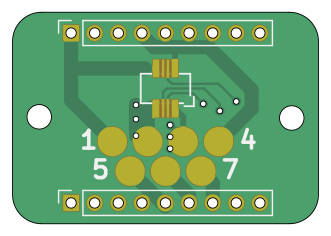
We will show everything on a single board located in
docs/resources/conn.kicad_pcb. The board looks like this when rendered via
PcbDraw:
Basic panels & layout
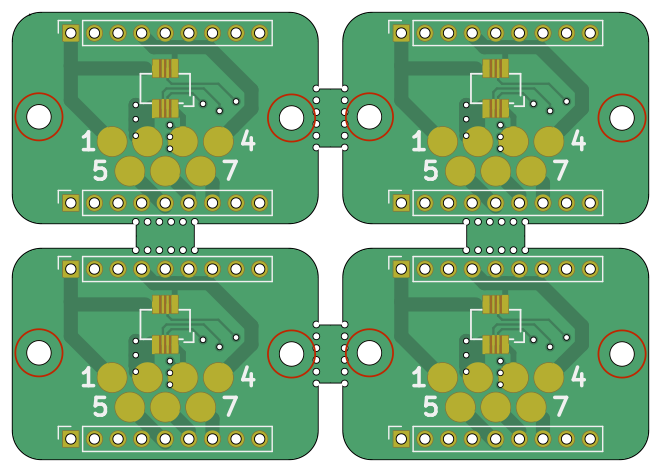
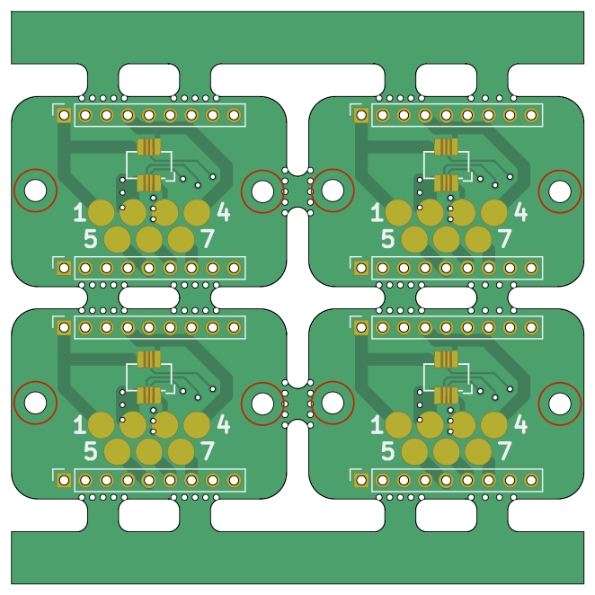
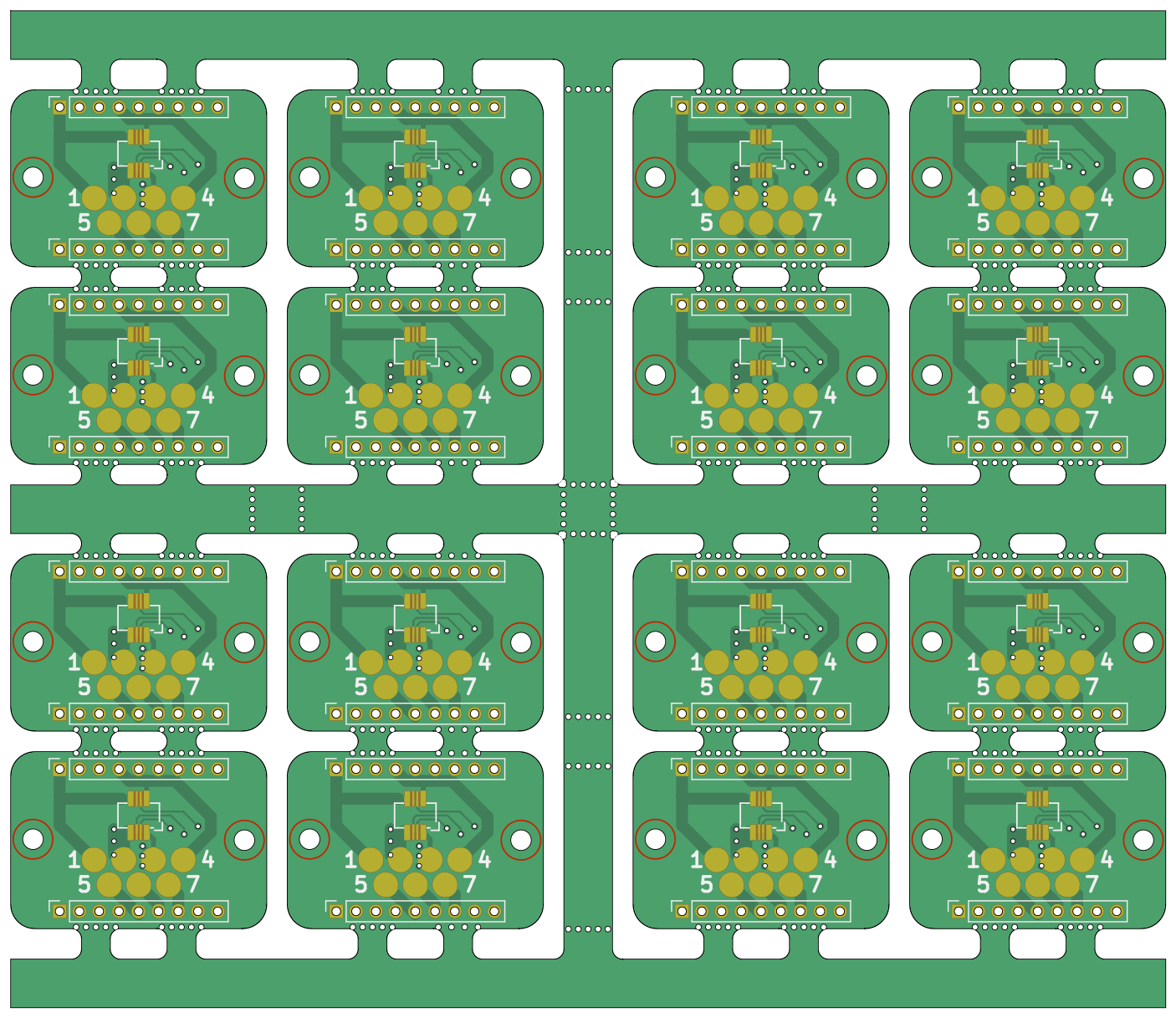
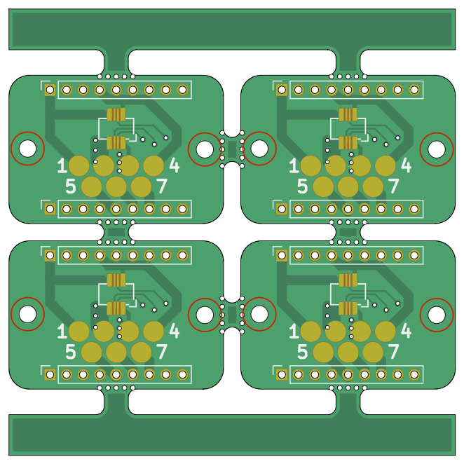
Let's start with our first panel.
Panelization command
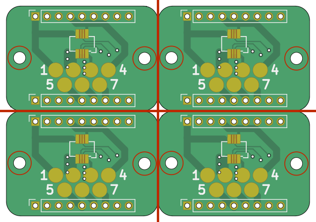
We specified that we want 2x2 panel, no space between board and separate them by V-cuts. We also specified that we want to build full tabs (although no tabs are visible in this example). This is ,however, essential – if we omitted tabs, no cuts between the boards would be performed. Note, that due to the rounded corners, this panel cannot be manufactured. We will fix it later.
Note that the \ in the input is there to make shell happy, so we can break our
command into multiple lines. Also note that there are single quotes around the
key-value pair – again, to make shell happy and to interpret a string with
spaces as a single option.
Note that on Windows you have the enter the commands into KiCAD Command Prompt instead of the regular Command Prompt. You can find it under the Start menu.
Also note that KiKit accepts all options in categories (e.g., layout, tabs,
cuts, ...). You can specify the parameters as a semicolon-separated key-value
list. To learn about the precise syntax of the CLI and about all options, please
refer to – documentation.
One side note – if you try it with your own board some components might be gone. KiKit respects the KiCAD component selection criteria. When you specify an input rectangle, only the components that fully fit inside the input rectangle are selected. This however take in account both name and value labels (even when they are hidden).
When you do not specify the source are explicitly, KiKit takes the board outline bounding box as the source area. Therefore, by default, components outside the board substrate are not copied to panel.
Note that this is intended behavior; for once it is consistent with KiCAD behavior of user selection and also it allows to easily ignore surrounding comments and drawings in the board sheet (it makes no sense to have 12 same copies of the notes around the board).
How to include the missing components?
- specify the source area explicitly to include all your components
- specify --source 'tolerance: 10mm' to enlarge the board outline bounding box
by e.g. 10 mm. The default value is 1 mm.
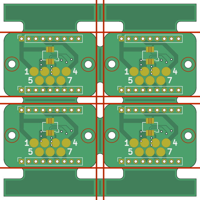
I told you that the panel above is not suitable for manufacturing. Let's see why:
Panelization command
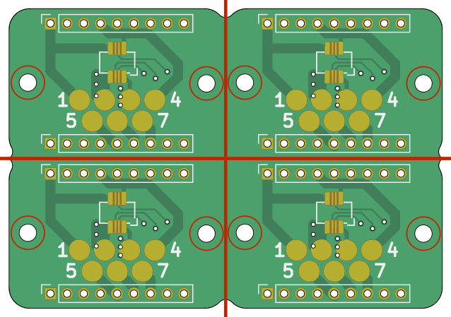
We specified a milling simulation post-processing. This simulates the milling operation in the fab house. As you can see, the sharp internal corners cannot be manufactured. I recommend you to use milling postprocessing always – you can easily see if your cuts are off or you have too narrow slots in your design.
Usually, one would use full tabs only for rectangular boards. Usually, when you have rounded corners, you will use short tabs instead and add some space between the boards. So let's fix it:
Panelization command
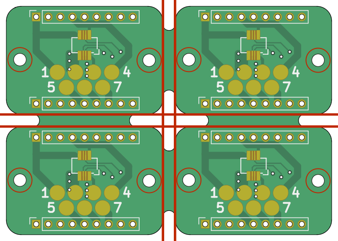
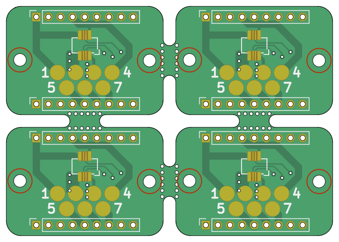
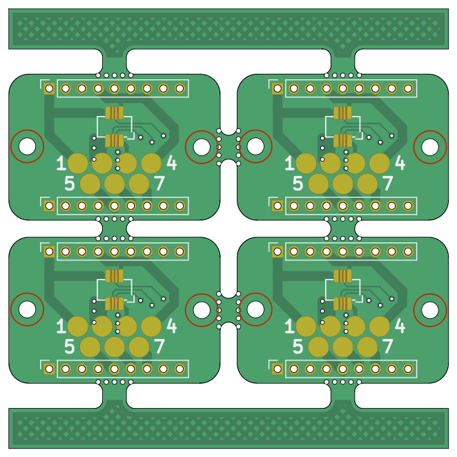
In that way, the rounded corners can be machined. Lets' see the same example with mousebites instead:
Panelization command
We changed cut type to mousebites and we specified that they should be
performed by 0.5mm holes with a spacing of 1 mm. You could also use inches if
you want – just specify `
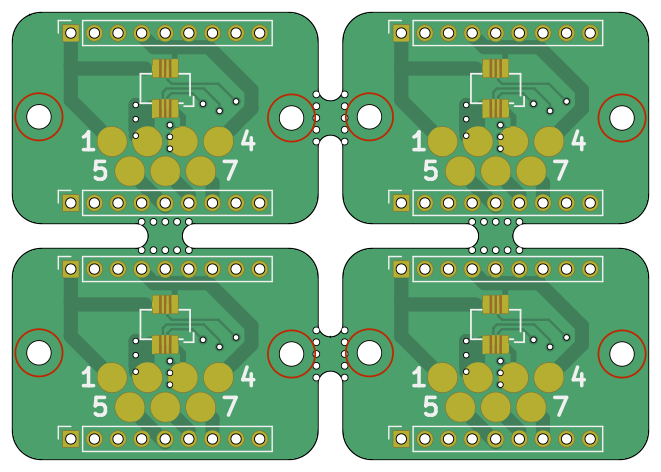
What happens, when we simulate the milling operation?
Panelization command
See? The cuts are somewhat short. This is due to the internal corners that cannot be milled. KiKit can fix that for you – just specify you want to prolong your cuts tangentially by a small amount:
Panelization command
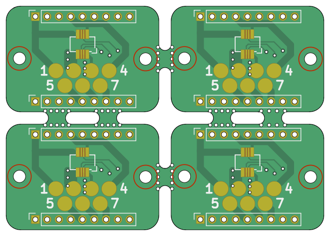
If you want, you can also specify a number of tabs to generate. KiKit will place them evenly:
Panelization command
You can also append frame or rails to the panel. Frames and rail are useful in the following situations:
- you want to assemble your board, so you need tooling holes, fiducial.
- you want to append a text to board (e.g., to identify a manufacturing batch)
- your boards are not rectangluar and you want to use V-Cuts (most manufactures require the outer edge of the panel to be a rectangle in order to manufacture V-Cuts)
Let's start with rails:
Panelization command
kikit panelize \
    --layout 'grid; rows: 2; cols: 2; space: 2mm' \
    --tabs 'fixed; width: 3mm; vcount: 2' \
    --cuts 'mousebites; drill: 0.5mm; spacing: 1mm; offset: 0.2mm; prolong: 0.5mm' \
    --framing 'railstb; width: 5mm; space: 3mm;' \
    --post 'millradius: 1mm' \
    docs/resources/conn.kicad_pcb panel.kicad_pcb
kikit panelize ^
    --layout "grid; rows: 2; cols: 2; space: 2mm" ^
    --tabs "fixed; width: 3mm; vcount: 2" ^
    --cuts "mousebites; drill: 0.5mm; spacing: 1mm; offset: 0.2mm; prolong: 0.5mm" ^
    --framing "railstb; width: 5mm; space: 3mm;" ^
    --post "millradius: 1mm" ^
    docs/resources/conn.kicad_pcb panel.kicad_pcb
Similarly, you can add left and right rail via the railslr type. If you want
a full frame, use the type frame. When you place a full frame, it might make
sense to include cuts in the corner of the frame, so you can break it apart
easily. Let's see an example:
Panelization command
kikit panelize \
    --layout 'grid; rows: 2; cols: 2; space: 2mm' \
    --tabs 'fixed; width: 3mm; vcount: 2' \
    --cuts 'mousebites; drill: 0.5mm; spacing: 1mm; offset: 0.2mm; prolong: 0.5mm' \
    --framing 'frame; width: 5mm; space: 3mm; cuts: both' \
    --post 'millradius: 1mm' \
    docs/resources/conn.kicad_pcb panel.kicad_pcb
kikit panelize ^
    --layout "grid; rows: 2; cols: 2; space: 2mm" ^
    --tabs "fixed; width: 3mm; vcount: 2" ^
    --cuts "mousebites; drill: 0.5mm; spacing: 1mm; offset: 0.2mm; prolong: 0.5mm" ^
    --framing "frame; width: 5mm; space: 3mm; cuts: both" ^
    --post "millradius: 1mm" ^
    docs/resources/conn.kicad_pcb panel.kicad_pcb
Note that you can also use just only a vertical or horizontal frame cuts:
Panelization command
kikit panelize \
    --layout 'grid; rows: 2; cols: 2; space: 2mm' \
    --tabs 'fixed; width: 3mm; vcount: 2' \
    --cuts 'mousebites; drill: 0.5mm; spacing: 1mm; offset: 0.2mm; prolong: 0.5mm' \
    --framing 'frame; width: 5mm; space: 3mm; cuts: h' \
    --post 'millradius: 1mm' \
    docs/resources/conn.kicad_pcb panel.kicad_pcb
kikit panelize ^
    --layout "grid; rows: 2; cols: 2; space: 2mm" ^
    --tabs "fixed; width: 3mm; vcount: 2" ^
    --cuts "mousebites; drill: 0.5mm; spacing: 1mm; offset: 0.2mm; prolong: 0.5mm" ^
    --framing "frame; width: 5mm; space: 3mm; cuts: h" ^
    --post "millradius: 1mm" ^
    docs/resources/conn.kicad_pcb panel.kicad_pcb
When you use V-cuts it might make sense to not remove all material, but only
mill a slot around the board of the board. This yields a stronger panel – and
some manufacturers require such style for assembly with V-Cuts. This is achieved
via framing type tightframe. Note that it does not make much sense with
mousebites.
Panelization command
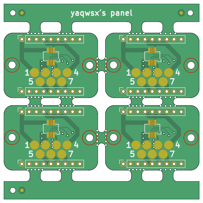
Once we have a frame, we can append a tooling holes, fiducials and some text to it:
Panelization command
kikit panelize \
    --layout 'grid; rows: 2; cols: 2; space: 2mm' \
    --tabs 'fixed; width: 3mm; vcount: 2' \
    --cuts 'mousebites; drill: 0.5mm; spacing: 1mm; offset: 0.2mm; prolong: 0.5mm' \
    --framing 'railstb; width: 5mm; space: 3mm;' \
    --tooling '3hole; hoffset: 2.5mm; voffset: 2.5mm; size: 1.5mm' \
    --fiducials '3fid; hoffset: 5mm; voffset: 2.5mm; coppersize: 2mm; opening: 1mm;' \
    --text 'simple; text: yaqwsx's panel; anchor: mt; voffset: 2.5mm; hjustify: center; vjustify: center;' \
    --post 'millradius: 1mm' \
    docs/resources/conn.kicad_pcb panel.kicad_pcb
kikit panelize ^
    --layout "grid; rows: 2; cols: 2; space: 2mm" ^
    --tabs "fixed; width: 3mm; vcount: 2" ^
    --cuts "mousebites; drill: 0.5mm; spacing: 1mm; offset: 0.2mm; prolong: 0.5mm" ^
    --framing "railstb; width: 5mm; space: 3mm;" ^
    --tooling "3hole; hoffset: 2.5mm; voffset: 2.5mm; size: 1.5mm" ^
    --fiducials "3fid; hoffset: 5mm; voffset: 2.5mm; coppersize: 2mm; opening: 1mm;" ^
    --text "simple; text: yaqwsx's panel; anchor: mt; voffset: 2.5mm; hjustify: center; vjustify: center;" ^
    --post "millradius: 1mm" ^
    docs/resources/conn.kicad_pcb panel.kicad_pcb
If you want to add text to both rails, you can use section --text2 to add a
second text. You can also use variables enclosed in curly brackets ({}). The
list of supported variables is listed in the documentation. Also, plugins can
introduce new variables.
Panelization command
kikit panelize \
    --layout 'grid; rows: 2; cols: 2; space: 2mm' \
    --tabs 'fixed; width: 3mm; vcount: 2' \
    --cuts 'mousebites; drill: 0.5mm; spacing: 1mm; offset: 0.2mm; prolong: 0.5mm' \
    --framing 'railstb; width: 5mm; space: 3mm;' \
    --tooling '3hole; hoffset: 2.5mm; voffset: 2.5mm; size: 1.5mm' \
    --fiducials '3fid; hoffset: 5mm; voffset: 2.5mm; coppersize: 2mm; opening: 1mm;' \
    --text 'simple; text: yaqwsx's panel; anchor: mt; voffset: 2.5mm; hjustify: center; vjustify: center;' \
    --text2 'simple; text: Created on {date}; anchor: mb; voffset: -2.5mm; hjustify: center; vjustify: center;' \
    --post 'millradius: 1mm' \
    docs/resources/conn.kicad_pcb panel.kicad_pcb
kikit panelize ^
    --layout "grid; rows: 2; cols: 2; space: 2mm" ^
    --tabs "fixed; width: 3mm; vcount: 2" ^
    --cuts "mousebites; drill: 0.5mm; spacing: 1mm; offset: 0.2mm; prolong: 0.5mm" ^
    --framing "railstb; width: 5mm; space: 3mm;" ^
    --tooling "3hole; hoffset: 2.5mm; voffset: 2.5mm; size: 1.5mm" ^
    --fiducials "3fid; hoffset: 5mm; voffset: 2.5mm; coppersize: 2mm; opening: 1mm;" ^
    --text "simple; text: yaqwsx's panel; anchor: mt; voffset: 2.5mm; hjustify: center; vjustify: center;" ^
    --text2 "simple; text: Created on {date}; anchor: mb; voffset: -2.5mm; hjustify: center; vjustify: center;" ^
    --post "millradius: 1mm" ^
    docs/resources/conn.kicad_pcb panel.kicad_pcb
There are many options for text and fiducials. Be sure to read the full documentation.
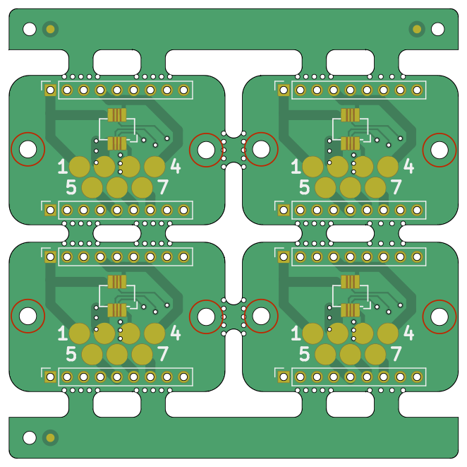
If you have an automatic feeder in your PNP machine or you just dislike sharp corners, you can add a chamfer or a fillet to the panel frame/rails:
Panelization command
kikit panelize \
    --layout 'grid; rows: 2; cols: 2; space: 2mm' \
    --tabs 'fixed; width: 3mm; vcount: 2' \
    --cuts 'mousebites; drill: 0.5mm; spacing: 1mm; offset: 0.2mm; prolong: 0.5mm' \
    --framing 'railstb; width: 5mm; space: 3mm; fillet: 1mm' \
    --tooling '3hole; hoffset: 2.5mm; voffset: 2.5mm; size: 1.5mm' \
    --fiducials '3fid; hoffset: 5mm; voffset: 2.5mm; coppersize: 2mm; opening: 1mm;' \
    --post 'millradius: 1mm' \
    docs/resources/conn.kicad_pcb panel.kicad_pcb
kikit panelize ^
    --layout "grid; rows: 2; cols: 2; space: 2mm" ^
    --tabs "fixed; width: 3mm; vcount: 2" ^
    --cuts "mousebites; drill: 0.5mm; spacing: 1mm; offset: 0.2mm; prolong: 0.5mm" ^
    --framing "railstb; width: 5mm; space: 3mm; fillet: 1mm" ^
    --tooling "3hole; hoffset: 2.5mm; voffset: 2.5mm; size: 1.5mm" ^
    --fiducials "3fid; hoffset: 5mm; voffset: 2.5mm; coppersize: 2mm; opening: 1mm;" ^
    --post "millradius: 1mm" ^
    docs/resources/conn.kicad_pcb panel.kicad_pcb
Panelization command
kikit panelize \
    --layout 'grid; rows: 2; cols: 2; space: 2mm' \
    --tabs 'fixed; width: 3mm; vcount: 2' \
    --cuts 'mousebites; drill: 0.5mm; spacing: 1mm; offset: 0.2mm; prolong: 0.5mm' \
    --framing 'railstb; width: 5mm; space: 3mm; chamfer: 1mm' \
    --tooling '3hole; hoffset: 2.5mm; voffset: 2.5mm; size: 1.5mm' \
    --fiducials '3fid; hoffset: 5mm; voffset: 2.5mm; coppersize: 2mm; opening: 1mm;' \
    --post 'millradius: 1mm' \
    docs/resources/conn.kicad_pcb panel.kicad_pcb
kikit panelize ^
    --layout "grid; rows: 2; cols: 2; space: 2mm" ^
    --tabs "fixed; width: 3mm; vcount: 2" ^
    --cuts "mousebites; drill: 0.5mm; spacing: 1mm; offset: 0.2mm; prolong: 0.5mm" ^
    --framing "railstb; width: 5mm; space: 3mm; chamfer: 1mm" ^
    --tooling "3hole; hoffset: 2.5mm; voffset: 2.5mm; size: 1.5mm" ^
    --fiducials "3fid; hoffset: 5mm; voffset: 2.5mm; coppersize: 2mm; opening: 1mm;" ^
    --post "millradius: 1mm" ^
    docs/resources/conn.kicad_pcb panel.kicad_pcb
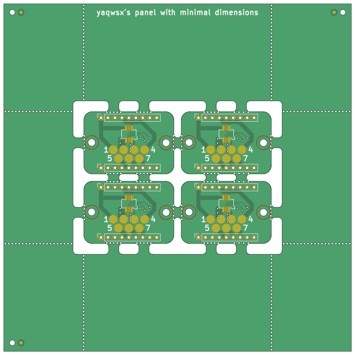
Some services, e.g., JLC PCB require a minimal panel size. If you want to ensure that your panel meets the criteria, you can specify minimal total width/height of the panel. Let's see an example:
Panelization command
kikit panelize \
    --layout 'grid; rows: 2; cols: 2; space: 2mm' \
    --tabs 'fixed; width: 3mm; vcount: 2' \
    --cuts 'mousebites; drill: 0.5mm; spacing: 1mm; offset: 0.2mm; prolong: 0.5mm' \
    --framing 'frame; width: 5mm; space: 3mm; mintotalheight: 100mm; mintotalwidth: 100mm' \
    --tooling '3hole; hoffset: 2.5mm; voffset: 2.5mm; size: 1.5mm' \
    --fiducials '3fid; hoffset: 5mm; voffset: 2.5mm; coppersize: 2mm; opening: 1mm;' \
    --text 'simple; text: yaqwsx's panel with minimal dimensions; anchor: mt; voffset: 2.5mm; hjustify: center; vjustify: center;' \
    --post 'millradius: 1mm' \
    docs/resources/conn.kicad_pcb panel.kicad_pcb
kikit panelize ^
    --layout "grid; rows: 2; cols: 2; space: 2mm" ^
    --tabs "fixed; width: 3mm; vcount: 2" ^
    --cuts "mousebites; drill: 0.5mm; spacing: 1mm; offset: 0.2mm; prolong: 0.5mm" ^
    --framing "frame; width: 5mm; space: 3mm; mintotalheight: 100mm; mintotalwidth: 100mm" ^
    --tooling "3hole; hoffset: 2.5mm; voffset: 2.5mm; size: 1.5mm" ^
    --fiducials "3fid; hoffset: 5mm; voffset: 2.5mm; coppersize: 2mm; opening: 1mm;" ^
    --text "simple; text: yaqwsx's panel with minimal dimensions; anchor: mt; voffset: 2.5mm; hjustify: center; vjustify: center;" ^
    --post "millradius: 1mm" ^
    docs/resources/conn.kicad_pcb panel.kicad_pcb
Advanced features & layouts
It is possible that you have some critical features you want to avoid with tabs. KiKit has several features that can help you. Let's start with the simple ones.
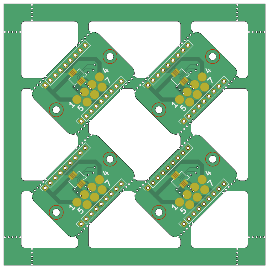
First, you can rotate the boards in your layout. This might make not much sense for rectanglar boards, but it might save you when you have circular or oddly shaped boards:
Panelization command
kikit panelize \
    --layout 'grid; rows: 2; cols: 2; space: 0mm; rotation: 45deg;' \
    --tabs 'fixed; width: 3mm;' \
    --cuts 'mousebites; drill: 0.5mm; spacing: 1mm; offset: 0.2mm; prolong: 0.75mm' \
    --framing 'frame; width: 5mm; space: 3mm; cuts: both' \
    --post 'millradius: 1mm' \
    docs/resources/conn.kicad_pcb panel.kicad_pcb
kikit panelize ^
    --layout "grid; rows: 2; cols: 2; space: 0mm; rotation: 45deg;" ^
    --tabs "fixed; width: 3mm;" ^
    --cuts "mousebites; drill: 0.5mm; spacing: 1mm; offset: 0.2mm; prolong: 0.75mm" ^
    --framing "frame; width: 5mm; space: 3mm; cuts: both" ^
    --post "millradius: 1mm" ^
    docs/resources/conn.kicad_pcb panel.kicad_pcb
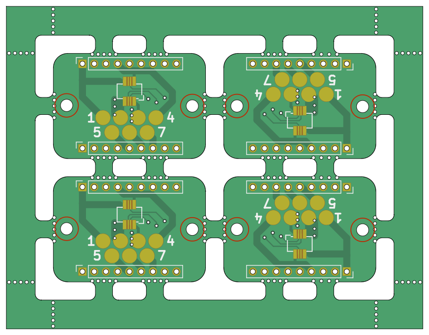
When your board has a connector sticking one one side of the board, it makes
sense to rotate the boards every other column, row or combination of both. KiKit
supports this via layout option alternation. You should be careful about
component references when rotating boards – KiCAD's references have a property
"Stay upright" which makes them always face up (even when placed on a panel). So
be sure to turn it off before panelizing. Here's an example:
Panelization command
kikit panelize \
    --layout 'grid; rows: 2; cols: 2; space: 3mm; alternation: cols;' \
    --tabs 'fixed; width: 3mm; vcount: 2' \
    --cuts 'mousebites; drill: 0.5mm; spacing: 1mm; offset: 0.2mm; prolong: 0.5mm' \
    --framing 'frame; width: 5mm; space: 3mm; cuts: both' \
    --post 'millradius: 1mm' \
    docs/resources/conn.kicad_pcb panel.kicad_pcb
kikit panelize ^
    --layout "grid; rows: 2; cols: 2; space: 3mm; alternation: cols;" ^
    --tabs "fixed; width: 3mm; vcount: 2" ^
    --cuts "mousebites; drill: 0.5mm; spacing: 1mm; offset: 0.2mm; prolong: 0.5mm" ^
    --framing "frame; width: 5mm; space: 3mm; cuts: both" ^
    --post "millradius: 1mm" ^
    docs/resources/conn.kicad_pcb panel.kicad_pcb
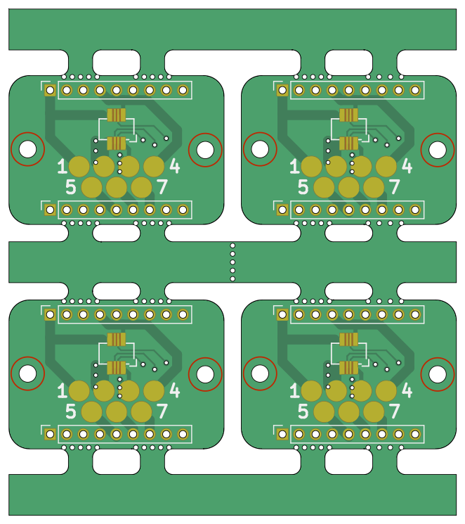
Another solution might be to not put tabs on, e.g., vertical edges of the PCB. However, in that case your panel might be weak for further assembly. You can make it more stiff by including backbones – a full piece of substrate between the panels. You can add either vertical, horizontal or both backbones. Also, similarly with frames, you can put cuts on your backbone to make depanelization of your boards easier. Enough theory, let's see an example
Panelization command
kikit panelize \
    --layout 'grid; rows: 2; cols: 2; space: 2mm; hbackbone: 5mm; hbonecut: true' \
    --tabs 'fixed; width: 3mm; vcount: 2; hcount: 0' \
    --cuts 'mousebites; drill: 0.5mm; spacing: 1mm; offset: 0.2mm; prolong: 0.5mm' \
    --framing 'railstb; width: 5mm; space: 3mm;' \
    --post 'millradius: 1mm' \
    docs/resources/conn.kicad_pcb panel.kicad_pcb
kikit panelize ^
    --layout "grid; rows: 2; cols: 2; space: 2mm; hbackbone: 5mm; hbonecut: true" ^
    --tabs "fixed; width: 3mm; vcount: 2; hcount: 0" ^
    --cuts "mousebites; drill: 0.5mm; spacing: 1mm; offset: 0.2mm; prolong: 0.5mm" ^
    --framing "railstb; width: 5mm; space: 3mm;" ^
    --post "millradius: 1mm" ^
    docs/resources/conn.kicad_pcb panel.kicad_pcb
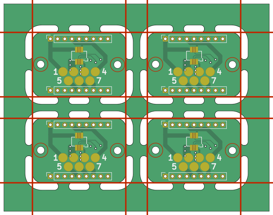
Often, not all backbones are needed. Especially for larger panels. Therefore, if you want, you can skip some of them. Consider the following 4×4 panel with only ever other backbone:
Panelization command
kikit panelize \
    --layout 'grid; rows: 4; cols: 4; space: 2mm; hbackbone: 5mm; vbackbone: 5mm; hboneskip: 1; vboneskip: 1' \
    --tabs 'fixed; width: 3mm; vcount: 2; hcount: 0' \
    --cuts 'mousebites; drill: 0.5mm; spacing: 1mm; offset: 0.2mm; prolong: 0.5mm' \
    --framing 'railstb; width: 5mm; space: 3mm;' \
    --post 'millradius: 1mm' \
    docs/resources/conn.kicad_pcb panel.kicad_pcb
kikit panelize ^
    --layout "grid; rows: 4; cols: 4; space: 2mm; hbackbone: 5mm; vbackbone: 5mm; hboneskip: 1; vboneskip: 1" ^
    --tabs "fixed; width: 3mm; vcount: 2; hcount: 0" ^
    --cuts "mousebites; drill: 0.5mm; spacing: 1mm; offset: 0.2mm; prolong: 0.5mm" ^
    --framing "railstb; width: 5mm; space: 3mm;" ^
    --post "millradius: 1mm" ^
    docs/resources/conn.kicad_pcb panel.kicad_pcb
The most powerful feature of KiKit regarding tab placement are tabs via annotation. Remember our test board? When you open it in Pcbnew, you can see that there are some special footprints – KiKit's annotations:
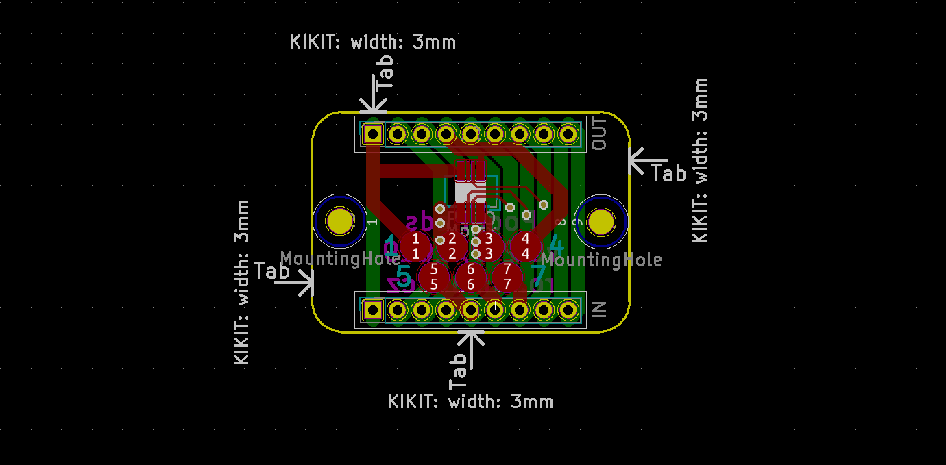
They specify where to place tabs. You can even specify individual tab width via
text property of the symbol. How to use it? Just specify tab type to
annotation. We also have to increase the source area tolerance, so it can
capture the annotations.
Panelization command
kikit panelize \
    --layout 'grid; rows: 2; cols: 2; space: 5mm;' \
    --tabs annotation \
    --source 'tolerance: 15mm' \
    --cuts 'mousebites; drill: 0.5mm; spacing: 1mm; offset: 0.2mm; prolong: 0.5mm' \
    --framing 'railstb; width: 5mm; space: 3mm;' \
    --post 'millradius: 1mm' \
    docs/resources/conn.kicad_pcb panel.kicad_pcb
kikit panelize ^
    --layout "grid; rows: 2; cols: 2; space: 5mm;" ^
    --tabs annotation ^
    --source "tolerance: 15mm" ^
    --cuts "mousebites; drill: 0.5mm; spacing: 1mm; offset: 0.2mm; prolong: 0.5mm" ^
    --framing "railstb; width: 5mm; space: 3mm;" ^
    --post "millradius: 1mm" ^
    docs/resources/conn.kicad_pcb panel.kicad_pcb
Well, the panel looks strange – right? That's because KiKit always constructs a half-bridges. When you specify the tabs location, you have to either ensure they match or put a piece of substrate they can reach – e.g., a backbone or a tightframe. If you are interested in the details, read more about tabs in section Understanding tabs. Let's fix it:
Panelization command
kikit panelize \
    --layout 'grid; rows: 2; cols: 2; space: 2mm; hbackbone: 3mm; vbackbone: 3mm' \
    --tabs annotation \
    --source 'tolerance: 15mm' \
    --cuts 'mousebites; drill: 0.5mm; spacing: 1mm; offset: 0.2mm; prolong: 0.5mm' \
    --framing 'railstb; width: 5mm; space: 3mm;' \
    --post 'millradius: 1mm' \
    docs/resources/conn.kicad_pcb panel.kicad_pcb
kikit panelize ^
    --layout "grid; rows: 2; cols: 2; space: 2mm; hbackbone: 3mm; vbackbone: 3mm" ^
    --tabs annotation ^
    --source "tolerance: 15mm" ^
    --cuts "mousebites; drill: 0.5mm; spacing: 1mm; offset: 0.2mm; prolong: 0.5mm" ^
    --framing "railstb; width: 5mm; space: 3mm;" ^
    --post "millradius: 1mm" ^
    docs/resources/conn.kicad_pcb panel.kicad_pcb
Note that the annotation can have an arbitrary orientation. The arrow just must be outside board edge and points towards it. KiKit will also place only those tabs, that have a neighboring substrate. For precise algorithm, see section understanding tabs.
When you make flex PCBs or you want to save etchant, it make sense to pour
copper on all non-functional parts of the panel. It will make the PCB rigid. You
can do so via copperfill section:
Panelization command
kikit panelize \
    --layout 'grid; rows: 2; cols: 2; space: 2mm' \
    --tabs 'fixed; width: 3mm;' \
    --cuts 'mousebites; drill: 0.5mm; spacing: 1mm; offset: 0.2mm; prolong: 0.5mm' \
    --framing 'railstb; width: 5mm; space: 3mm;' \
    --copperfill solid \
    --post 'millradius: 1mm;' \
    docs/resources/conn.kicad_pcb panel.kicad_pcb
kikit panelize ^
    --layout "grid; rows: 2; cols: 2; space: 2mm" ^
    --tabs "fixed; width: 3mm;" ^
    --cuts "mousebites; drill: 0.5mm; spacing: 1mm; offset: 0.2mm; prolong: 0.5mm" ^
    --framing "railstb; width: 5mm; space: 3mm;" ^
    --copperfill solid ^
    --post "millradius: 1mm;" ^
    docs/resources/conn.kicad_pcb panel.kicad_pcb
When you use V-cuts with copperfill you (or your fab house) might want to
include a clearance around the V-cuts:
Panelization command
If you, for example do not wish to cover the tabs with copper, you can also specify clearance. Also, some manufacturers don't like when you have large solid copper areas. In that case, you can use a hatch pattern to fill the area:
Panelization command
kikit panelize \
    --layout 'grid; rows: 2; cols: 2; space: 2mm' \
    --tabs 'fixed; width: 3mm;' \
    --cuts 'mousebites; drill: 0.5mm; spacing: 1mm; offset: 0.2mm; prolong: 0.5mm' \
    --framing 'railstb; width: 5mm; space: 3mm;' \
    --copperfill 'hatched; clearance: 2mm; spacing: 0.5mm; width: 0.5mm' \
    --post 'millradius: 1mm;' \
    docs/resources/conn.kicad_pcb panel.kicad_pcb
kikit panelize ^
    --layout "grid; rows: 2; cols: 2; space: 2mm" ^
    --tabs "fixed; width: 3mm;" ^
    --cuts "mousebites; drill: 0.5mm; spacing: 1mm; offset: 0.2mm; prolong: 0.5mm" ^
    --framing "railstb; width: 5mm; space: 3mm;" ^
    --copperfill "hatched; clearance: 2mm; spacing: 0.5mm; width: 0.5mm" ^
    --post "millradius: 1mm;" ^
    docs/resources/conn.kicad_pcb panel.kicad_pcb
Note one last facts about V-cuts. V-cuts can only be straight and
horizontal/vertical. But you can use them with circular boards if you want by
cutting a little inside them. The option cutcurves, that will approximate the
cut by staring and ending point.
I would like... but KiKit does not support it!
If you need something special; e.g., custom placement of tooling holes, multiple texts, etc. KiKit has you covered.
The CLI interface allows you to run a custom script over the final panel. The script can use KiKit Python interface to modify it. For the sake of simplicity, let's add a hole in the middle of the frame. Therefore, we write the following script:
from kikit.units import mm
from kikit.common import toKiCADPoint

def kikitPostprocess(panel, arg):
    minx, miny, maxx, maxy = panel.panelBBox()
    position = toKiCADPoint(((minx + maxx) // 2, miny + 2 * mm))
    panel.addNPTHole(position, 3 * mm)
Then run KiKit:
Panelization command
kikit panelize \
    --layout 'grid; rows: 2; cols: 2; space: 2mm' \
    --tabs 'fixed; width: 3mm; vcount: 2' \
    --cuts 'mousebites; drill: 0.5mm; spacing: 1mm; offset: 0.2mm; prolong: 0.5mm' \
    --framing 'railstb; width: 5mm; space: 3mm;' \
    --post 'millradius: 1mm; script: docs/resources/examplePost.py' \
    docs/resources/conn.kicad_pcb panel.kicad_pcb
kikit panelize ^
    --layout "grid; rows: 2; cols: 2; space: 2mm" ^
    --tabs "fixed; width: 3mm; vcount: 2" ^
    --cuts "mousebites; drill: 0.5mm; spacing: 1mm; offset: 0.2mm; prolong: 0.5mm" ^
    --framing "railstb; width: 5mm; space: 3mm;" ^
    --post "millradius: 1mm; script: docs/resources/examplePost.py" ^
    docs/resources/conn.kicad_pcb panel.kicad_pcb
You can learn more about available functions from the comment in the source code or in the Python API reference. The basic concepts are summarized in the scripting guide.
If you implement a feature that your fab house requires (e.g., new tooling hole type), consider submitting a pull request for KiKit instead. I believe the others will benefit from it.
Managing presets
The last section of this document is dedicated to management of presets. You can read the specification in the documentation for CLI. Here I would like to focus on practical examples.
As you should know from the documentation, the panelization preset is divided
into sections; e. g., layout, tabs, etc. The key-value parameters in these
sections can be specified via JSON files. In KiKit, you can specify these files
via -p option:
kikit panelize -p myPreset.json -p :<builtInPreset> <other parameters>
The parameters in the later specified presets override the parameters in the
previously specified presets. This allows you to define a named piece-wise
presets. Therefore, you can prepare various presets for mousebites – e.g.,
fineMousebites.json and coarseMousebites.json:
// fineMousebites.json
{
    "cuts": {
        "type": "mousebites", "drill": "0.5mm", "spacing": "0.9mm", "offset":
        "0.25mm"
    }
}

// coarseMousebites.json
{
    "cuts": {
        "type": "mousebites", "drill": "0.3mm", "spacing": "0.2mm", "offset":
        "0.15mm"
    }
}
Then you can specify your panelization commands easily via:
kikit panelize -p fineMousebites.json <otheroptions>
Therefore, you can build a custom library of commonly used-options; e.g., per
fabrication house. KiKit offers some built-in presets – see
panelizePresets.
Note that the built-in preset default.json is always used as a base and it
specifies conservative default values so you can only override the options
relevant for you.
To give you an example – with KiKit, you will no longer have to remember what diameter of tooling holes JLC PCB requires, just use:
kikit panelize -p :jlcTooling <otheroptions>